
Google has widened its eighth-generation TPU lineup with TPU 8tx, a confidential computing accelerator, and TPU 8i Max, a dual-chip inference package for long-context work. For UK buyers wary of a single-vendor AI stack, both give a genuine alternative route to NVIDIA DGX systems.
View the data behind this chart
| TPU 8i | TPU 8i Max | |
|---|---|---|
| On-chip SRAM | 384 MB | 768 MB |
Four TPU systems in one year — what actually shipped
Google says this is the first year it has introduced four distinct TPU systems, and the latest two are not new silicon but new packaging around existing chips. TPU 8tx reuses TPU 8t silicon with a confidential computing shell built around it, while TPU 8i Max fuses two TPU 8i chips onto a single package. Google credits its modular approach, altering packaging, memory, networking and security around a fixed chip, with letting it ship specialised configurations in months rather than a full silicon cycle.
Google says TPUs now have nearly 100 customers, spanning frontier AI labs, trading firms, retailers and universities. Google says some customers can now deploy TPUs directly in their own data centres; it has not said that TPU 8tx or TPU 8i Max is available for such deployments. Neither TPU 8tx nor TPU 8i Max has a stated Google Cloud availability date or published price, which matters for anyone trying to budget a 2027 deployment today.
TPU 8tx: confidential computing as a built-in feature, not a bolt-on
TPU 8tx pairs TPU 8t's accelerator silicon with 5th Generation AMD EPYC host CPUs and bakes in confidential computing hardware features: PCIe link encryption, cryptographic attestation and secure memory enclaves, so data and model weights stay isolated while in use rather than only at rest or in transit. Google positions TPU 8tx for regulated enterprises and governments running frontier or proprietary models and agents alongside sensitive data.
It also inherits the low-latency Boardfly network built for TPU 8i, which Google says gives TPU 8tx up to 2x lower latency than plain TPU 8t with a near-zero performance penalty. Google says TPU 8tx is intended to support fine-tuning, distillation and reinforcement-learning agent training without moving sensitive data between separate clusters.
TPU 8i Max: memory bandwidth for agents and long context
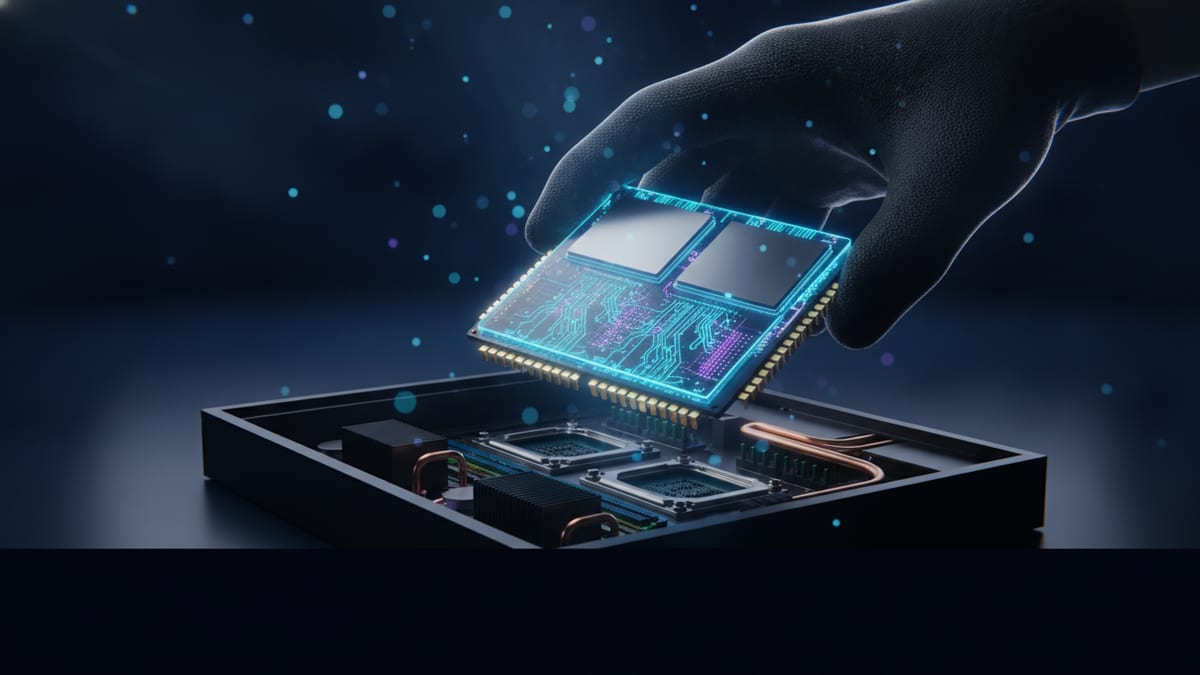
TPU 8i Max doubles compute, on-chip SRAM and HBM bandwidth over a single TPU 8i by putting two of those chips on one package. Google lists 384MB of SRAM for TPU 8i; doubling that gives 768MB per TPU 8i Max package, within the same rack footprint. TPU 8i has 384MB of SRAM; because 8i Max combines two chips, Google describes the package as having twice the SRAM—768MB by calculation. Google positions this for workloads such as dozens of agents operating across an entire codebase or hours of video, where memory bandwidth, not raw compute, is the bottleneck. Because it fits twice the silicon into an unchanged rack envelope, Google is also selling it on compute density per square foot and per watt, a line item that matters directly for UK data centre operators facing power and space constraints.
The UK sovereignty and Nvidia-alternative angle
Google maps the four systems to workload roles: TPU 8t for scale-up training, TPU 8i for low-latency reasoning, TPU 8tx for confidential computing, and TPU 8i Max for large context windows and rack density. That gives UK buyers building out UK sovereign AI repatriation strategies a Google-designed alternative to Nvidia-based confidential AI infrastructure, subject to availability and deployment constraints, relevant given that Nvidia has proposed an NVL72 security domain spanning Rubin GPUs, Vera CPUs and interconnects, while Intel is also working to extend TDX toward trusted I/O for accelerator data paths.
Google's decision to run the confidential path through AMD EPYC hosts rather than its usual Arm-based hosts is notable in itself: it hands AMD a seat in the trusted-computing chain of a hyperscale AI system even though Google still designs the accelerator silicon. For procurement teams comparing platforms, that is one more data point that the comparison is becoming multi-vendor, although the competing offerings differ in maturity and availability.
Software underneath: TPU Sync, Pathways, and dynamic slicing
The hardware news arrives alongside several software moves relevant to reliability and operating cost. TPU Sync, now open source, treats chip HBM, host DRAM, shared storage and the data centre network as one memory hierarchy. Google says TPU Sync cuts KV-cache transfer latency by more than 90% and reduces time to first token by an average of 90% on open-weight MoE models with 235B–480B parameters. Google says Cloud Pathways is generally available on GKE and supports sub-minute slice hot-swapping and elastic resharding during hardware disruptions, and GKE dynamic slicing uses optical circuit switching to reshape TPU topologies without rebuilding node pools. Google says GKE dynamic slicing can cut job startup times by up to 5x and speed fault recovery by up to 4.5x. For teams scoping infrastructure for dedicated inference rather than training, these operational claims are arguably as important as the new chip packages themselves.
View the data behind this chart
| Primary Role | Key Feature | Best For | |
|---|---|---|---|
| TPU 8t | Scale-up training | Pod to 9,600 chips | Large-model pretraining |
| TPU 8i | Low-latency reasoning | Boardfly network | Real-time inference |
| TPU 8tx | Confidential inference | AMD EPYC + enclaves | Regulated data workloads |
| TPU 8i Max | Long-context inference | 768MB SRAM, dual chip | Agent and video workloads |
What UK buyers should do before committing
Google has not published pricing or a Google Cloud availability date for either system; buyers should confirm availability directly. The immediate action is diligence, not procurement. Buyers should map current workloads against the four-way TPU 8 split, check whether a workload genuinely needs data-in-use protection (TPU 8tx) versus raw context and density (TPU 8i Max), and keep the comparison honest against Nvidia and Intel confidential-computing roadmaps rather than assuming TPU is the default. Running the numbers through tools such as Servnet's AI GPU sizing calculator alongside the AI servers data study will help separate marketing claims from workload reality before any server configuration decisions are locked in for 2027 budgets.
- 01StorageReview — Google Adds Confidential TPU 8tx and Dual-Chip TPU 8i Max to Its Eighth-Generation TPU Lineup · 13 November 2026
- 02Data Center Dynamics — Google expands eighth-generation TPU portfolio with two new TPU systems · 10 November 2026
- 03Tom's Hardware — Google adds two new specialized chips for AI agents and security to 8th-gen TPU lineup · 10 November 2026
- 04ServeTheHome — Google TPU 8tx and 8i Max use AMD EPYC Turin · 11 November 2026
- 05The Next Platform — Google rejiggers TPU accelerators for broader AI inference work · 9 November 2026
- 06storagereview.com
- 07tomshardware.com
- 08theregister.com